Rick's b.log - entry 2017/05/12 |
| ||||||
mailto: blog -at- heyrick -dot- eu
You are not reading my b.log using HTTPS. You can switch to HTTPS by clicking here. Neuros OSD test pointsI had written most of this before I got ill. A brief tidy of the markup, and here it is... A list of the test points on the Neuros OSD board.
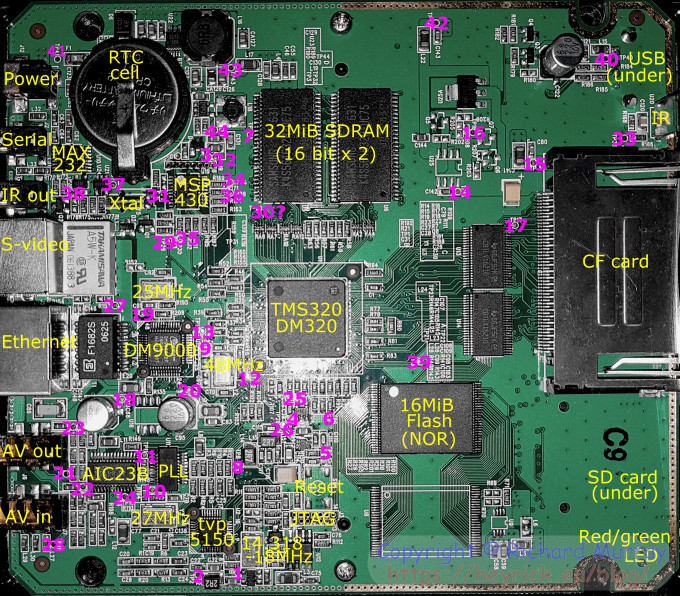
Here are the DM320 GPIO assignments: GPIO00 IN MSP430 IRQ GPIO01 ? Pulled low, but has TP6 GPIO03 IN MSP430 IR IRQ GPIO05 IN MS card detect GPIO06 IN Ethernet IRQ GPIO07 OUT USB power enable GPIO08 IN SD card detect GPIO09 IN CF card detect GPIO10 OUT TVP5150 PDN (power down) GPIO12 OUT PLL FS1 GPIO16 OUT LED red GPIO17 OUT LED green GPIO25 OUT CF enable GPIO27 IN Serial RxD GPIO28 OUT Serial TxD GPIO29 OUT CF power enable GPIO30 BI IIC clock GPIO31 BI IIC data GPIO32 OUT Enable video GPIO33 OUT 80kHz GPIO34 OUT Blaster signal (PWM) GPIO35 IN SD write protect GPIO36 OUT CF reset GPIO37 OUT CF STSCHG GPIO40 IN? TVP5150 C_WEN (active video area)
Your comments:Please note that while I check this page every so often, I am not able to control what users write; therefore I disclaim all liability for unpleasant and/or infringing and/or defamatory material. Undesired content will be removed as soon as it is noticed. By leaving a comment, you agree not to post material that is illegal or in bad taste, and you should be aware that the time and your IP address are both recorded, should it be necessary to find out who you are. Oh, and don't bother trying to inline HTML. I'm not that stupid! ☺ ADDING COMMENTS DOES NOT WORK IF READING TRANSLATED VERSIONS.
  
(Felicity? Marte? Find out!)
📺 The SIBA stories 📹
It's a simple substring match.
Last read at 05:03 on 2024/05/02.


| ||||||||||||||||||||||||||||||||||||||||||||||||||||||||||||||||||||||||||||||||||||||||||||||||||||||||||||||||||||||||||||||||||||||||||||
| Next entry - 2017/05/13 Return to top of page |
| © 2017 Rick Murray |
| Retrieved from http://heyrick.eu/blog/index.php?diary=20170512 on 2nd May 2024 |