It is the 1729th of March 2020 (aka the 23rd of November 2024)
You are 3.135.194.138,
pleased to meet you!
mailto:blog-at-heyrick-dot-eu
DSO 138 - analogue input
Since I don't currently have a DSO138 to build, I will look at the schematic and explain what's going on. To be honest, the oscilloscope is really rather simple in hardware, with the smarts being contained within the non-open source part of the firmware.
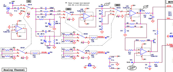
Here is the analogue input part of the schematic:
It contains the most components, but then there's not a lot else asides from some buttons and the power conditioning.
Don't panic, we'll work through it bit by bit. You don't need to try to read that stuff above.
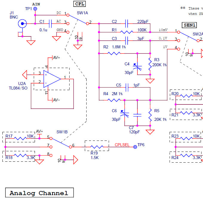
The BNC socket, on the far left, is the signal input. The signal that is delivered to the oscilloscope is selected by SW1A. It operates in three modes. The first is DC coupling, which is a direct connection between the input and the 'scope. The second is AC coupling where the signal is taken by way of capacitor C1. This has the function of stripping any DC component from a waveform, so the waveform delivered to the rest of the hardware will be oscillating around zero, not the DC value. The final option is for GND coupling. In this case, the incoming waveform is disconnected and the input signal is tied to ground. This is usually used to set up the oscilloscope, as it provides you with a known 0V reference.
The switch used to select the coupling mode is a variety with two sets of poles. The first set of poles are used as described above. The second set, SW1B, which you can see at the bottom of the drawing, are used to report the switch status to the microcontroller.
Following the coupling, there is a section of circuit to deal with the sensitivity of the input signal. A simple resistor/capacitor deals with the 10mV sensitivity. Some more complex hardware, and larger resistor values, are required for the 0.1V and 1V ranges. These larger ranges also have variable capacitors for trimming the circuit response at higher frequencies. What is interesting, as it may be out of the cost bracket or build capabilities, is that those two capacitors are the only adjustable components. There is no other calibration, so I do wonder if the device is showing a waveform at, say, 3.7V, how accurate this would actually be. Plus, of course, whether or not the readings are liable to drift with ambient temperature.
As before, the switch is dual poles, with the second poles reporting the switch position back to the microcontroller.
The input signal from the sensitivity selection is connected to a TL084 Operational Amplifier (op-amp for short). If you look carefully, you will see that the output (pin 7) is corrected back as one of the inputs (pin 6). This means the op-amp is working as a "voltage follower". The purpose of this is to act as a buffer to try to eliminate loading effects due to an impedance mismatch.
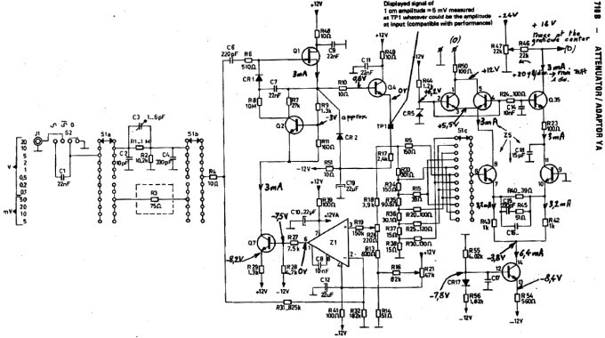
Why is this important? Because as much as we might like to take accurate measurements, the very act of measuring will affect that which is being measured. So the aim here is to have as little as possible on the input (and thus connected to the original circuit). Looking at the schematics, is a simpler but not so different version of that which handles the input of my OX710B oscilloscope (picture below).
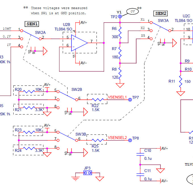
Following this, another three way switch that is part of a passive attenuator which offers a direct connection for ×1 (where at the 1V sensitivity, one square on the screen will equal 1V in reality), through a resistor for the ×2 range (where at 1V sensitivity, one square equals 2V), or through two resistors for the ×5 range (at 1V sens, a square on the screen equals 5V). Accordingly, the most that the oscilloscope can cope with is an input of 50V (ten squares, 1V ×5...; though this may in reality be +/- 25V from zero).
As always, the switch is dual, with the second set of poles for reporting status to the microcontroller.
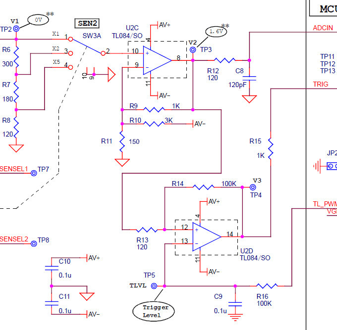
The signal leaves the ×1/×2/×5 attenuator and passes into a non-inverting amplifier (another part of the TL084). In this case, the signal is not only boosted, but it is shifted so that the 0V on the input becomes 1.6V on the output. This is because the analogue to digital convertor within the microcontroller is only capable of dealing with signals in the range 0V to ~3.8V. Accordingly, 0V input is +1.6V, meaning that +3.8V is maximum positive and 0V is maximum negative.
Of course, there are liable to be accuracy issues when measuring at the ×5 range, considering that the greatest voltage swing that the microcontroller will ever see is ~3.8V. At the 1V ×5 setting, the difference between one volt and another will be approximately 0.064V. That said, if the ADC genuinely manages 1024 levels of sampling accuracy, that means each sample would represent 0.0037V, so it should be capable of working down to a twentieth of a volt even at maximum range - though whether or not other tolerances affect that will remain to be seen.
Of course, it is worth noting that this is a kit that costs in the £20 / $30 / €20 range (prices vary greatly), so one shouldn't expect to compare this kit to a big expensive proper oscilloscope.
All of that being said, it would seem prudent to correctly set the switches prior to connecting any sort of input. I do not know if any of the op-amps provide clamping, or if pushing 20V into the device at the 10mV ×1 setting would deliver something extremely unpleasant to the microcontroller. I'm going to suggest that this may, in fact, turn out to be the case, and it won't do kind things to the ADC. So always check the input settings carefully before connecting an input signal.
The input signal goes though some simple final conditioning before being presented to the microcontroller as ADCIN.
You will notice there's an extra part to this circuit. A third part of the TL084 is used to control the automatic triggering. Being used as a comparator, the op-amp accepts a trigger threshold from the microcontroller and compares it with the signal being presented on the input. If the conditions match, a TRIG signal is created which is sent to the microcontroller to initiate sampling.
And that...is that.
By way of example, here is the schematic for one of the inputs of my OX710B. You will notice some similarities.
Your comments:
Please note that while I check this page every so often, I am not able to control what users write; therefore I disclaim all liability for unpleasant and/or infringing and/or defamatory material. Undesired content will be removed as soon as it is noticed. By leaving a comment, you agree not to post material that is illegal or in bad taste, and you should be aware that the time and your IP address are both recorded, should it be necessary to find out who you are. Oh, and don't bother trying to inline HTML. I'm not that stupid! ☺ ADDING COMMENTS DOES NOT WORK IF READING TRANSLATED VERSIONS.
You can now follow comment additions with the comment RSS feed. This is distinct from the b.log RSS feed, so you can subscribe to one or both as you wish.
David Pilling, 28th December 2016, 02:23
Often the ADC inputs have diodes to the power supply rails, take them outside the power supply range and they clamp. That might be what R12 is doing, limiting current.
AJK, 2nd July 2018, 17:40
I had trouble understanding the SW1, SW2, SW3 switch type. Are they 8-pin ON-ON-ON Single Pole Triple Throw ? DP3T?
This web page is licenced for your personal, private, non-commercial use only. No automated processing by advertising systems is permitted.
RIPA notice: No consent is given for interception of page transmission.